
www.magazine-industry-usa.com
26
'26
Written on Modified on
Inline Wafer Thickness Measurement in Confined Environments
Micro-Epsilon introduces a robust interferometric sensor enabling precise inline thickness measurement of silicon and silicon carbide wafers in high-contamination production processes.
www.micro-epsilon.com
Accurate thickness measurement of semiconductor wafers during processing remains critical for yield and quality control, particularly in grinding and lapping operations. A new interferometric sensor design addresses this requirement by enabling stable, inline measurement of silicon (Si) and silicon carbide (SiC) wafers under demanding environmental conditions.
Design for constrained and contaminated production settings
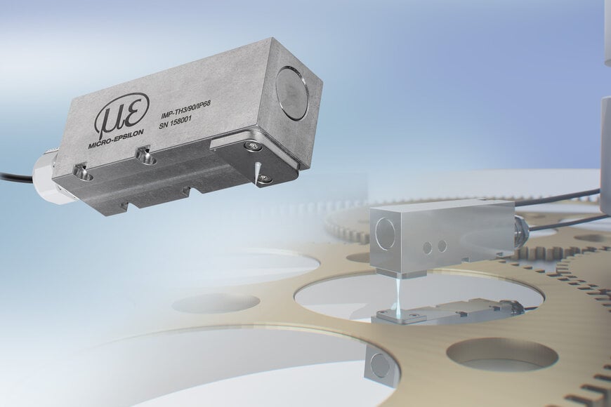
The sensor is engineered for integration directly into production equipment where space is limited and exposure to moisture and particles is high. A 90° beam path allows flexible optical alignment in confined installation environments, while a short working distance of 3 mm supports placement close to the measurement target. This configuration enables inline deployment without requiring significant modifications to existing machinery.
To maintain measurement reliability in processes such as slurry grinding, the sensor is housed in an IP68-rated stainless steel enclosure. This level of protection ensures resistance to water ingress and particulate contamination, allowing operation in wet and abrasive environments typically associated with wafer thinning and surface finishing.
Maintaining signal stability during grinding processes
In grinding and lapping applications, optical contamination can significantly degrade measurement accuracy. The sensor incorporates an integrated air purge system designed to continuously remove particles from the optical path. This mechanism helps maintain consistent signal quality by preventing debris accumulation on optical components.
The optical setup generates a small measurement spot with a diameter of 15 µm, supporting high-resolution thickness detection even on highly doped wafers. This is particularly relevant in semiconductor manufacturing, where material properties and surface conditions can affect signal reflectivity and measurement precision.
Application in semiconductor manufacturing
Inline thickness measurement is essential in semiconductor wafer processing to ensure uniformity and prevent defects that may impact downstream device performance. The sensor is designed to operate with a dedicated controller, forming a compact measurement system suitable for integration into automated production lines.
Typical application areas include:
- Wafer grinding and thinning processes
- Lapping and polishing operations
- Inline quality control in semiconductor fabrication
By enabling stable measurements under high contamination and limited space conditions, the system supports process optimization and contributes to improved yield in semiconductor manufacturing environments.
Edited by Romila DSilva, Induportals Editor, with AI assistance.
Edited by Romila DSilva, Induportals Editor, with AI assistance.
