
www.magazine-industry-usa.com
21
'18
Written on Modified on
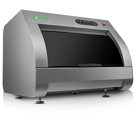
New XRF Instrument Measures the Smallest Features in Semiconductor. Microelectronics Manufacturing
Bowman’s W Series uses poly-capillary optics to focus the X-ray beam to 7.5 µm FWHM, the world’s smallest beam size for coating thickness analysis using XRF technology. A 150X magnification camera is used to measure features on that scale; it is accompanied by a secondary, low-magnification camera for live-viewing samples and birds-eye macro-view imaging. Bowman’s dual-camera system lets operators see the entire part, click the image to zoom with the high-mag camera, and pinpoint the feature to be programmed and measured.
A programmable X-Y stage with precision less than +/- 1 µm for each axis is used to select and measure multiple points; Bowman pattern recognition software and auto-focus features also do this automatically. The system’s 3D mapping capability can be used to view the topography of a coating on a part such as a silicon wafer.
The W Series is the 7th model in Bowman’s XRF instrument suite.
The W Series uses poly-capillary optics to focus the X-ray beam to 7.5 µm FWHM, the world’s smallest beam size for coating thickness analysis using XRF technology. A 150X magnification camera is used to measure features on that scale; it is accompanied by a secondary, low-magnification camera for live-viewing samples and birds-eye macro-view imaging. Bowman’s dual-camera system lets operators see the entire part, click the image to zoom with the high-mag camera, and pinpoint the feature to be programmed and measured.
A programmable X-Y stage with precision less than +/- 1 µm for each axis is used to select and measure multiple points; Bowman pattern recognition software and auto-focus features also do this automatically. The system’s 3D mapping capability can be used to view the topography of a coating on a part such as a silicon wafer.
The standard configuration of W Series instruments includes 7.5 µm optics with molybdenum anode tube (chromium and tungsten are optional) and a high-resolution, large-window Silicon Drift Detector which processes more than 2 million counts per second.
The W Series is the 7th model in Bowman’s XRF instrument suite. Like others in the portfolio, it simultaneously measures up to 5 coating layers and runs advanced Xralizer software to quantify coating thickness from the detected photons. Xralizer software combines intuitive visual controls with time-saving shortcuts, extensive search capability, and “one-click” reporting. The software also simplifies user creation of new applications.
www.bowmanxrf.com