
www.magazine-industry-usa.com
02
'25
Written on Modified on
IDS: See. Align. Place
Precision vision systems power Micro-LED bonding and HBM packaging.
en.ids-imaging.com
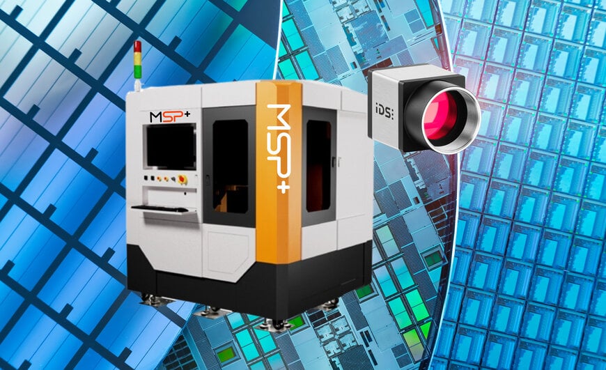
As miniaturization progresses and efficiency increases in micro LED displays and modern semiconductor components, precision and scalability in production are becoming decisive success factors. The Taiwanese company Micraft Systems Plus has developed two state-of-the-art systems to meet these challenges: the uLED Laser Soldering Machine and the HBM High-Accuracy Die Bonder. For both machines, the manufacturer relies on industrial cameras from the USB 3 uEye CP series from IDS Imaging Development Systems to ensure maximum accuracy, speed and process control. These systems are already in high-volume use across the Asian electronics market.
Application 1: Micro-LED Transfer & Laser Soldering with 20MP USB3 uEye CP cameras
The uLED Laser Soldering Machine enables precise high-speed soldering of micro LEDs onto large-area substrates - including G4.5 and G6 glass plates. Laser technology reduces thermal and mechanical stress and is therefore ideal for the simultaneous processing of thousands of tiny components.
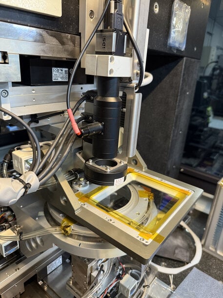
Automated production cell for high-precision die bonding with USB 3 uEye CP industrial camera from IDS for camera-based substrate alignment and quality control.
First, the cameras are used to capture global reference marks for the rough alignment or to determine the rough position of the substrate in the machine coordinate system. This position data is then transmitted to the motion control system, which enables high-precision motion control on this basis - with a repeat accuracy of the coordinates of around ±1 µm.
After successful qualification, the chips are aligned and transferred with the highest precision. For fine adjustment, the cameras now capture fiducial marks and thus enable real-time sub-micrometer alignment of the substrate and, if necessary, dynamic rotation correction. The alignment data determined is transferred to the motion control system, which adjusts the position and angle of the stage accordingly in order to place each micro-LED exactly at the target position. With a throughput rate of up to 10 million chips per hour, the system combines maximum precision with high processing efficiency - a decisive KPI for scalable series production.
This is followed by an inline inspection: The camera automatically moves to the relevant position so that the operator can carry out a visual check directly during the process - for example with regard to correct alignment, possible skewing, physical damage or placement errors.
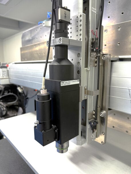
USB 3 uEye CP industrial cameras from IDS are the sharp eyes of the uLED laser soldering machine from MSP.
Camera technology for complex image processing tasks
USB 3 uEye CP cameras from IDS are the eyes of the uLED Laser Soldering Machine. Two integrated U3-3800CP-M-GL Rev.2.2 cameras perform several tasks in the process:
- Donor wafer inspection (during mass transfer): Detection of defects such as cracks or missing chips to select only functional micro-LEDs.
- Alignment & placement: Identification of markings and fiducials on substrates and dies, with transmission of precise coordinates to the motion system for exact positioning.
- Post-transfer inspection: Verification of chip positioning with regard to position, inclination and integrity.
- Repair & Rework: Support of pick-and-place systems for the targeted replacement of individual chips.
"The extremely high-resolution images with very low noise capture even the finest details," emphasizes Damien Wang, Area Sales Manager APAC South East at IDS. The integrated camera model is based on the Sony STARVIS CMOS sensor IMX183 with rolling shutter with a resolution of 20.44 MP (5536 × 3692 px) and 2.4 µm pixel size.
The camera therefore delivers up to 19.8 images per second and is ideal for demanding inspection tasks.
Application 2: Die Bonding for High Bandwidth Memory (HBM) with 12MP USB3 uEye CP cameras
The second system, the HBM High-Accuracy Die Bonder from the MCB series, is designed for state-of-the-art semiconductor packaging, in particular for High Bandwidth Memory (HBM), in which several chips are stacked vertically. Precision in the micrometer range is crucial here.
Two U3-3890CP-M-GL Rev.2.2 cameras from IDS localize the microchips and bonding pads, provide precise coordinates to the placement unit and enable the individual components to be placed accurately. "The IDS camera is also mainly used here for the alignment system in our HBM system. It identifies the positions of the chip and the target substrate and converts this information into coordinates for the motion control system in order to achieve precise positioning and alignment," explains the manufacturer. The control unit uses these coordinates to control placement with sub-micrometer accuracy, ensuring consistent results with high-density placements.
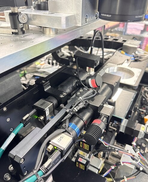
Two U3-3890CP-M-GL Rev.2.2 cameras from IDS identify the uLED chip location
The inline inspection checks each connection for placement accuracy, alignment integrity and possible damage. In high-density storage stacks, even the smallest deviations can lead to electrical or thermal problems - the demands on image processing are correspondingly high.
Sensor performance for precise die bonding
The U3-3890CP Rev.2.2 uses the Sony IMX226 rolling shutter CMOS sensor with 12 MP (4000 × 3000 px) and 1.85 µm pixel size. It is characterized by exceptional light sensitivity and low noise values. At full resolution, up to 33.2 fps are possible - ideal for fast, precise processes. Thanks to IDS camera integration, the system offers high repeat accuracy and long-term process stability - ideal for complex 2.5D and 3D packaging applications.
Computer vision for high-precision semiconductor production: uEye CP from IDS
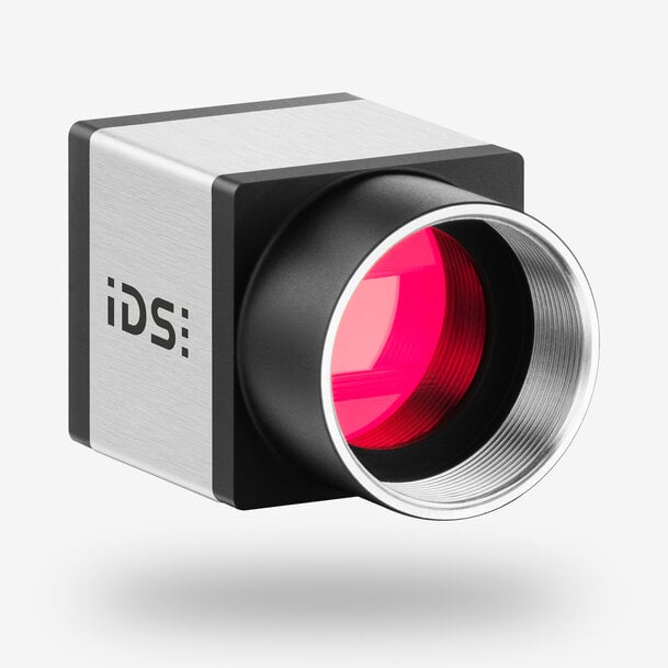
Both state-of-the-art systems from the Taiwanese manufacturer are based on the uEye CP series from IDS - compact industrial cameras (29 × 29 × 29 mm) with a robust magnesium housing, USB3 Vision connection and CMOS global or rolling shutter sensors from the Sony STARVIS series. Thanks to back-side illumination (BSI), they deliver razor-sharp, low-noise images even in low light - crucial for detecting the finest structural features, solder contacts and chip positions in the sub-micrometer range.
A key requirement for the cameras is that the fast frame rate and minimal latency ensure seamless interaction with motion control systems and provide real-time image data for quick adjustments. They also impress with their high reliability and are designed for continuous 24/7 operation - a decisive factor in semiconductor production. The standby mode reduces the power consumption in idle mode to a minimum and thus contributes to energy efficiency, making the industrial camera an environmentally friendly solution for long-term use.
With the comprehensive software SDK from IDS, the cameras can be easily integrated and calibrated on site - an important prerequisite for efficiency and precision in automated production environments.
Customer benefit: Scalable precision and increased efficiency
By integrating IDS camera technology into both platforms, Micraft Systems Plus was able to significantly increase process accuracy, repeatability and reliability. Error rates have been reduced, set-up times shortened and overall production efficiency improved - a clear competitive advantage for customers in the micro-LED and high-end semiconductor packaging sectors.
Both systems are already in use at leading electronics manufacturers in Taiwan and other Asian markets and are regarded as best-practice examples of the integration of German camera technology into state-of-the-art production solutions for micro-LED and semiconductor packaging.
Outlook
The market for precision automation is developing rapidly - and with it the demands on modern industrial cameras. "Now more than ever, our customers are demanding high-resolution, compact and absolutely reliable solutions," says Damien Wang. The trend towards higher resolution in particular is driving innovation: Razor-sharp, detailed images are essential for complex automation tasks. At the same time, stable performance is a basic requirement, even under difficult operating conditions. "Many applications require continuous, uninterrupted operation. That is why our focus is increasingly on cameras that work reliably even under demanding conditions," emphasizes the responsible project manager from Micraft Systems Plus. Another trend is the advancing miniaturization. Industrial cameras with compact designs are becoming increasingly important, as space in modern systems is often limited without compromising on performance.
To take account of these developments, the product portfolio is being systematically expanded and adapted to the increasing technical requirements.
Camera
uEye CP - incredibly fast, powerful, future-proof
Camera family: uEye CP
Models used:
U3-3800CP-M-GL Rev.2.2
U3-3890CP-M-GL Rev.2.2
The camera therefore delivers up to 19.8 images per second and is ideal for demanding inspection tasks.
Application 2: Die Bonding for High Bandwidth Memory (HBM) with 12MP USB3 uEye CP cameras
The second system, the HBM High-Accuracy Die Bonder from the MCB series, is designed for state-of-the-art semiconductor packaging, in particular for High Bandwidth Memory (HBM), in which several chips are stacked vertically. Precision in the micrometer range is crucial here.
Two U3-3890CP-M-GL Rev.2.2 cameras from IDS localize the microchips and bonding pads, provide precise coordinates to the placement unit and enable the individual components to be placed accurately. "The IDS camera is also mainly used here for the alignment system in our HBM system. It identifies the positions of the chip and the target substrate and converts this information into coordinates for the motion control system in order to achieve precise positioning and alignment," explains the manufacturer. The control unit uses these coordinates to control placement with sub-micrometer accuracy, ensuring consistent results with high-density placements.
Two U3-3890CP-M-GL Rev.2.2 cameras from IDS identify the uLED chip location
The inline inspection checks each connection for placement accuracy, alignment integrity and possible damage. In high-density storage stacks, even the smallest deviations can lead to electrical or thermal problems - the demands on image processing are correspondingly high.
Sensor performance for precise die bonding
The U3-3890CP Rev.2.2 uses the Sony IMX226 rolling shutter CMOS sensor with 12 MP (4000 × 3000 px) and 1.85 µm pixel size. It is characterized by exceptional light sensitivity and low noise values. At full resolution, up to 33.2 fps are possible - ideal for fast, precise processes. Thanks to IDS camera integration, the system offers high repeat accuracy and long-term process stability - ideal for complex 2.5D and 3D packaging applications.
Computer vision for high-precision semiconductor production: uEye CP from IDS
Both state-of-the-art systems from the Taiwanese manufacturer are based on the uEye CP series from IDS - compact industrial cameras (29 × 29 × 29 mm) with a robust magnesium housing, USB3 Vision connection and CMOS global or rolling shutter sensors from the Sony STARVIS series. Thanks to back-side illumination (BSI), they deliver razor-sharp, low-noise images even in low light - crucial for detecting the finest structural features, solder contacts and chip positions in the sub-micrometer range.
A key requirement for the cameras is that the fast frame rate and minimal latency ensure seamless interaction with motion control systems and provide real-time image data for quick adjustments. They also impress with their high reliability and are designed for continuous 24/7 operation - a decisive factor in semiconductor production. The standby mode reduces the power consumption in idle mode to a minimum and thus contributes to energy efficiency, making the industrial camera an environmentally friendly solution for long-term use.
With the comprehensive software SDK from IDS, the cameras can be easily integrated and calibrated on site - an important prerequisite for efficiency and precision in automated production environments.
Customer benefit: Scalable precision and increased efficiency
By integrating IDS camera technology into both platforms, Micraft Systems Plus was able to significantly increase process accuracy, repeatability and reliability. Error rates have been reduced, set-up times shortened and overall production efficiency improved - a clear competitive advantage for customers in the micro-LED and high-end semiconductor packaging sectors.
Both systems are already in use at leading electronics manufacturers in Taiwan and other Asian markets and are regarded as best-practice examples of the integration of German camera technology into state-of-the-art production solutions for micro-LED and semiconductor packaging.
Outlook
The market for precision automation is developing rapidly - and with it the demands on modern industrial cameras. "Now more than ever, our customers are demanding high-resolution, compact and absolutely reliable solutions," says Damien Wang. The trend towards higher resolution in particular is driving innovation: Razor-sharp, detailed images are essential for complex automation tasks. At the same time, stable performance is a basic requirement, even under difficult operating conditions. "Many applications require continuous, uninterrupted operation. That is why our focus is increasingly on cameras that work reliably even under demanding conditions," emphasizes the responsible project manager from Micraft Systems Plus. Another trend is the advancing miniaturization. Industrial cameras with compact designs are becoming increasingly important, as space in modern systems is often limited without compromising on performance.
To take account of these developments, the product portfolio is being systematically expanded and adapted to the increasing technical requirements.
Camera
uEye CP - incredibly fast, powerful, future-proof
Camera family: uEye CP
Models used:
U3-3800CP-M-GL Rev.2.2
U3-3890CP-M-GL Rev.2.2
